Hardware Design Guide
Overview#
If you are designing hardware using the WizFi360 please refer to this document.
This document includes a reference circuit diagram and a PCB guide.
Pin definition#
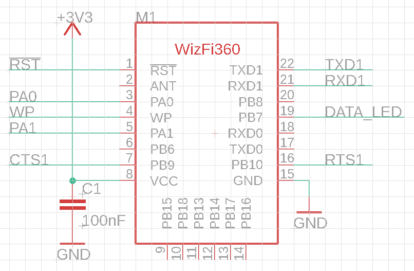
Figure 1. WizFi360 Pinout

Table 1. Pin Definitions
| Pin Name | Type | Pin Function |
|---|---|---|
| RST | I | Module Reset Pin (Active Low) |
| NC | - | WizFi360-PA Reserved |
| ANT | O | WizFi360-CON ANT pin for external antenna |
| PA0 | I/O | BOOT Pin (Active low) When power on or reset is low, it operates in Boot mode. In the normal operating mode, this pin can be controlled by AT command. |
| WP | I | WAKEUP Pin (Active High) If the wake-up pin is high in Standby mode, the WizFi360 is reset to the normal operating mode. |
| PA1 | I | Pull down over 3s for taking effect. UART1's current parameter changes to default value (please refer to the AT+UART_CUR command in WizFi360 AT command manual). |
| PB6 | I/O | This pin can be controlled by AT command. |
| PB9 | I | CTS Pin of UART1 If you don't use the CTS function, this pin can be controlled by AT command. |
| VCC | P | Power Pin (Typical Value 3.3V) |
| PB15 | I/O | This pin can be controlled by AT command. |
| PB18 | I/O | This pin can be controlled by AT command. |
| PB13 | I/O | This pin can be controlled by AT command. |
| PB14 | I/O | This pin can be controlled by AT command. |
| PB17 | I/O | This pin can be controlled by AT command. |
| PB16 | I/O | This pin can be controlled by AT command. |
| GND | I/O | Ground Pin |
| PB10 | O | RTS Pin of UART1 If you don't use the RTS function, this pin can be controlled by AT command. |
| TXD0 | O | TXD Pin of UART0 |
| RXD0 | I | RXD Pin of UART0 |
| PB7 | O | LED Light output (Active low). Go to Low while each TX/RX packet and then back to high. Note: It has been connected to onboard LED for WizFi360-PA |
| PB8 | I/O | This pin can be controlled by AT command. |
| RXD1 | I | RXD Pin of UART1 |
| TXD1 | O | TXD Pin of UART1 |
important
UART1 is used for AT command and data communication. UART0 is used for debugging and firmware upgrade.
Initial value of GPIO Pins#
This is the initial value of GPIO when using AT command to use GPIO on WizFi360.
| Pin Name | Type | Value | Pull up/down |
|---|---|---|---|
| PA0 | I/O | High | Pull up |
| PB6 | I/O | Low | Pull down |
| PB9 | I/O | Low | Pull down |
| PB15 | I/O | High | Pull down |
| PB18 | I/O | High | Pull down |
| PB13 | I/O | High | Pull down |
| PB14 | I/O | High | Pull down |
| PB17 | I/O | High | Pull down |
| PB16 | I/O | High | Pull down |
| PB10 | I/O | Low | Pull down |
| PB07 | I/O | High | Pull down |
| PB08 | I/O | High | Pull down |
Circuit#
System#
The WizFi360 has a very simple circuit. You can connect power to the WizFi360 and send and receive data through UART1. Please pay attention to four pins.
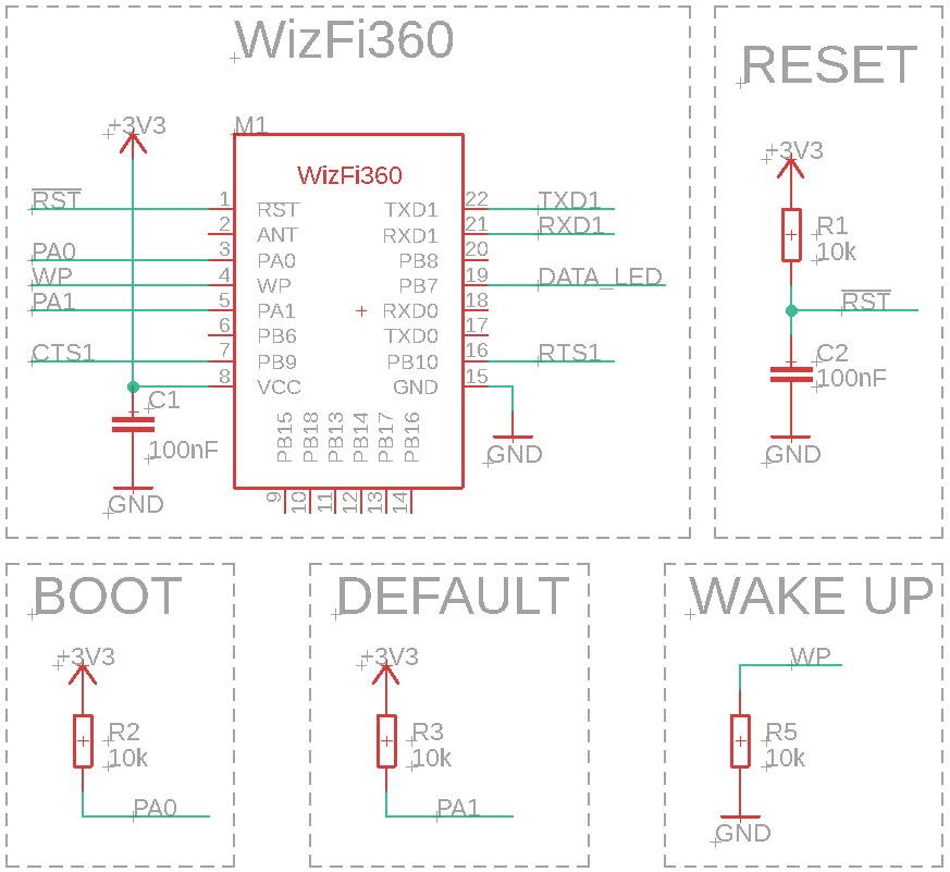
- Reset
Reset circuit offers to design with RC circuit. WizFi360 reset automatically by low level power. If RESET pin controlled by external circuit, the WizFi360 will reset when the level is below 2.0V. The low level needs to last more than 100µs. - PA0
PA0 circuit offers to design 10k pull-up. PA0 is used as a boot pin, but it's use unlikely for normal users. This pin is used at the factory stage. (Module production) - PA1
PA1 circuit offers to design 10k pull-up. If PA1 is Low for 3 seconds, UART1's current parameter changes to default value (please refer to the AT+UART_CUR command in WizFi360 AT command manual). - WP
WP circuit offers to design user configuration. You must control this pin if you are using standby mode. If this pin is high in Standby mode, the WizFi360 is reset to the normal operating mode.
Power#
WizFi360 requires the use of a power supply capable of supplying 3.0V to 3.6V and more than 500mA. Because WizFi360 operates normally from 3.0V to 3.6V, it consumes up to 230mA of instantaneous current. The wiring width should not be less than 30mil. The power stabilizing capacitor (100nF) should be placed close to the VCC pin.
UART#
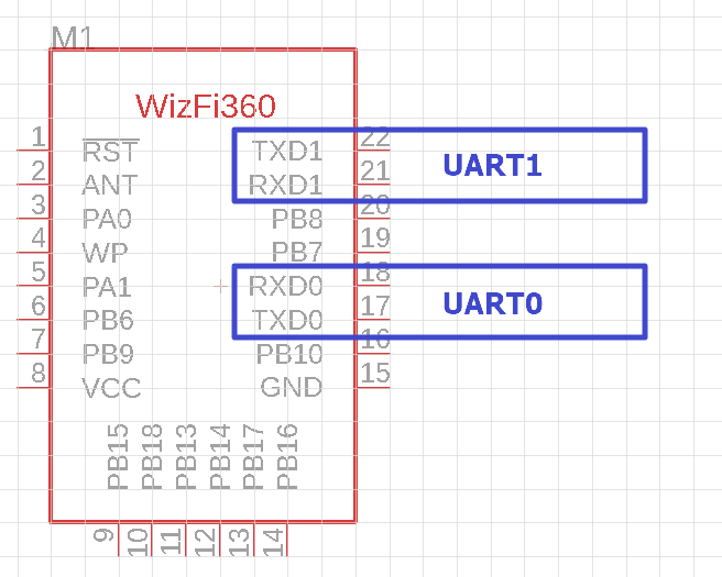
- UART1
UART1 is the main communication UART. AT command communication is possible with UART1 and data communication is possible. - UART0
UART0 is not available to normal users. This UART is used at the factory stage (Module production) and intended for internal firmware developers of the WizFi360.
ETC#
This session is an additional circuit guide for using the WizFi360. You don't have to keep this session. But if you need it, you design it.
- UART Flow Control
If you want to use UART Flow Control, you need to design a circuit as shown in Figure 3. PB9 is CTS1, PB10 is RTS1.
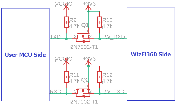
- UART Level Shifter
The UART voltage on the WizFi360 is 3.3V. However, your MCU may not have a voltage of 3.3V. If so you need a Level Shifter to connect the WizFi360 to your MCU. You can design a Level Shifter circuit by referring to Figure 4. Connect your MCU’s UART voltage to the VCCIO at Figure 4.
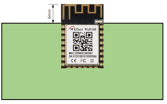
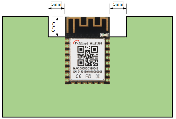
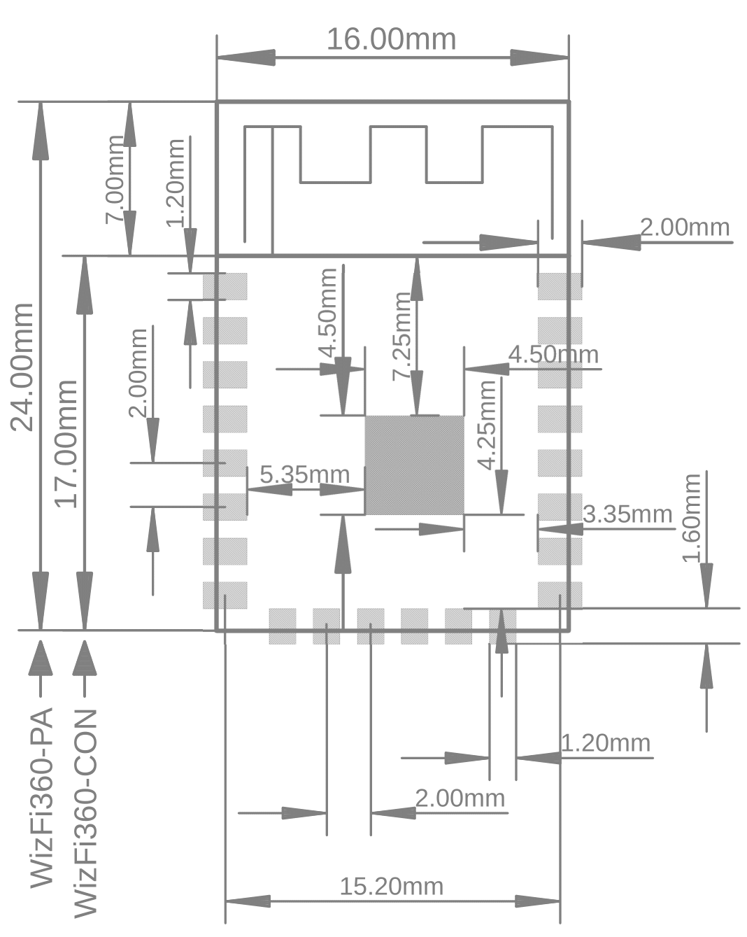
PCB Footprint#
PCB Layout#
- Power wiring width should not be less than 30mil.
- Except for the antenna portion of WizFi360, the bottom layer of the shield can must have a GND plane.
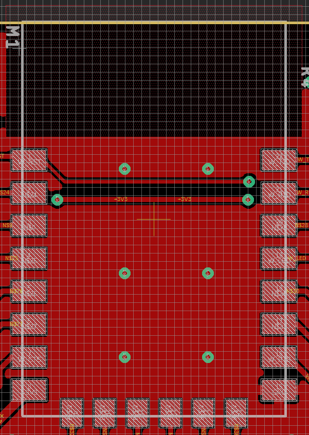
- Figures. 6 and Figures. 7 are 2 antenna placement which can best performance of antenna. We suggest customers to choose one of these 2 modes to design the placement. For the second placement mode, PCB antenna should be at least 5.0mm from both sides of the bottom board.